



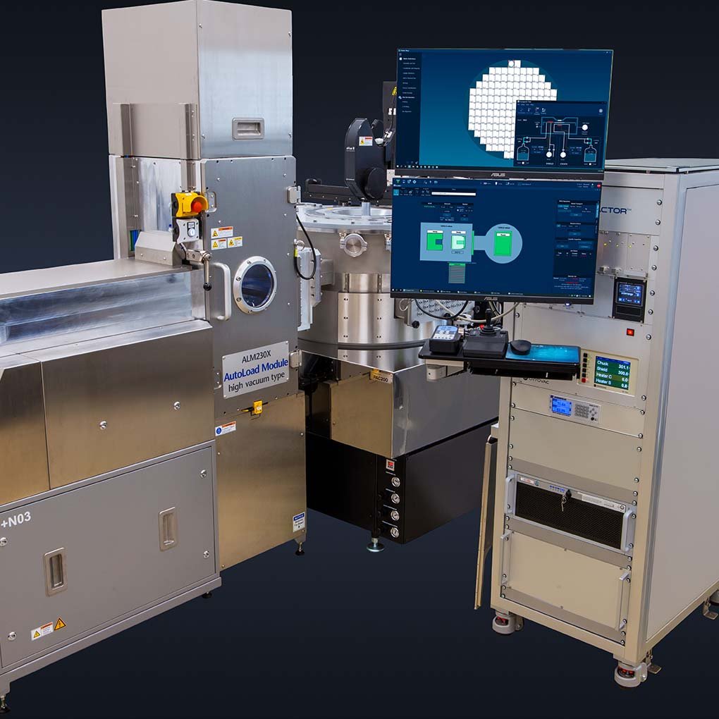
For many laboratories and research organizations, cryogenic wafer probing has traditionally been a highly manual process. Engineers often spend significant time loading wafers, cooling systems, collecting measurements, warming the chamber, and repeating the process for the next wafer.
That approach has worked well for years. But as research programs expand and more devices need to be characterized, manual testing is starting to slow everything down.
What truly sets the PAC200-auto probe system apart is its flexible carrier-based automation. Rather than being limited to handling full wafers, the system can accommodate a wide range of sample formats, e.g. full wafer, wafer pieces, or individual dies mounted on a carrier. This gives researchers the freedom to automate cryogenic testing for virtually any device configuration, making the PAC200-auto an ideal solution for both production-scale wafer characterization and early-stage research prototypes.
Why Cryogenic Testing Matters
Many of today’s most advanced semiconductor technologies have to be tested at cryogenic temperatures to fully understand how they’ll perform.
Researchers developing quantum processors, superconducting circuits, cryogenic CMOS, infrared detectors, photon detectors, and other advanced devices must understand how electrical characteristics change at extremely low temperatures.
Cryogenic wafer probing allows engineers to evaluate devices before packaging, helping teams identify issues earlier and move through design iterations more efficiently.
As these technologies become more sophisticated, however, the amount of testing required grows rapidly. Instead of evaluating a handful of prototype devices, organizations are increasingly testing complete wafers and multiple process iterations.
As testing volumes grow, the supporting test infrastructure has to grow with them.
The Challenge with Manual Cryogenic Wafer Probing
Traditional cryogenic probe stations deliver exceptional measurement capability, but many still rely on manual wafer loading and unloading.
For researchers, this often means:
- Interrupting measurement workflows to exchange wafers
- Spending valuable engineering time on repetitive handling tasks
- Reduced throughput during long characterization campaigns
- Greater opportunity for handling errors or process variability
Automation helps eliminate much of that repetitive work while still delivering the precision cryogenic measurements demand.
Bringing Automation to Cryogenic Wafer Testing
The PAC200-auto was designed specifically to bridge this gap. By combining an automated wafer loader with FormFactor’s established cryogenic probing platform, researchers can perform unattended wafer loading while maintaining the precise environmental control required for low-temperature device characterization.
The system supports:
- Fully-automated wafer handling
- Temperatures down to about 77 K using liquid nitrogen
- Temperatures down to about 10 K using liquid helium
- Optional dry-cooling configurations
- Wafer sizes up to 200 mm
- Probe cards and/or up to eight probe positioners
- Integration with multiple optical instruments, including infrared radiation sources (black bodies)
Instead of stopping to manually swap wafers throughout the day, researchers can run longer test sequences with less hands-on involvement.
Supporting the Next Generation of Quantum Research
The benefits become especially clear in quantum device development. Whether researchers are evaluating superconducting qubits, cryogenic control electronics, or quantum sensors, engineers need data from a large number of structures and process variations before they can confidently evaluate new designs.
As fabrication processes improve and device counts grow, researchers are expected to evaluate more devices than ever.
Automated cryogenic wafer probing helps laboratories:
- Characterize larger numbers of devices
- Improve repeatability across measurement runs
- Reduce operator intervention
- Increase laboratory productivity
- Make better use of expensive cryogenic equipment
Instead of spending valuable lab time loading wafers, engineers can focus on what really matters: analyzing results and improving their designs.
Built for More Than Quantum Computing
Quantum computing may be getting most of the attention today, but it isn’t the only application that relies on cryogenic measurements.
The PAC200-auto is equally well suited for research involving:
- Infrared imaging devices
- Superconducting electronics
- Cryogenic CMOS
- Single-photon detectors
- Space and defense sensor technologies
- Advanced semiconductor materials
Support for multiple optical instruments further expands the system’s flexibility for specialized research environments.
Increasing Throughput Without Compromising Precision
Every lab is trying to do the same thing: increase throughput without giving up measurement accuracy.
Automation makes that balance much easier to achieve.
The PAC200-auto delivers the same high-precision cryogenic probing environment researchers expect while reducing the manual effort associated with repetitive wafer handling. The result is a workflow that’s easier to manage, more productive for researchers, and a better use of expensive cryogenic test equipment.
As research programs transition from exploratory studies toward larger-scale device development, automated cryogenic wafer probing becomes an increasingly important part of building scalable test infrastructure.